Semiconductor Lithography Equipment - Market Share Analysis, Industry Trends & Statistics, Growth Forecasts (2026 - 2031)
半導体リソグラフィー装置市場は、タイプ(深紫外線リソグラフィーおよび極端紫外線リソグラフィー)、用途(高度パッケージング、MEMSデバイス、およびLEDデバイス)、および地域(北米、ヨーロッパなど)によって区分されています。
The Semiconductor Lithography Machine Manufacturers Market is Segmented by Type (Deep Ultraviolet Lithography and Extreme Ultraviolet Lithography), Application (Advanced Packaging, MEMS Devices, and LED Devices), and Geography (North America, Europe, and More).
| 出版 | Mordor Intelligence |
| 出版年月 | 2026年02月 |
| ページ数 | 123 |
| 価格 | 記載以外のライセンスについてはお問合せください |
| シングルユーザ | USD 4,750 |
| 種別 | 英文調査報告書 |
| 商品番号 | SMR-14522 |

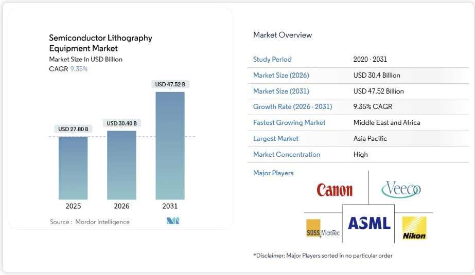
半導体リソグラフィー装置市場は、2025年の278億米ドルから2026年には304億米ドルに成長し、2031年には475.2億米ドルに達すると予測されています。この市場拡大の勢いは、極端紫外線(EUV)への移行と近々登場する高開口数(High-NA)EUVプラットフォーム、人工知能(AI)サーバーの急増、そしてより高密度なパターニング精度が求められる数兆トランジスタのグラフィックスアクセラレータに起因しています。アジア太平洋地域は、台湾のファウンドリ市場における優位性と韓国の4,710億米ドル規模のメガクラスター計画に牽引され、引き続き製造能力拡大の中心となっています。深紫外線(DUV)ツールは依然として成熟ノードの基盤となっていますが、高開口数(High-NA)EUVの受注パイプラインは、エコシステムが1nm未満の生産へと急速に移行していることを示しています。資本支出の集中と輸出管理の順守が普及の主な障害となっているが、政府の補助金、パッケージの革新、エネルギー効率の高いツールの設計が相まって、高度な露光システムの対応可能な基盤が拡大している。
セグメント分析
- 2025年には、DUVプラットフォームは半導体リソグラフィ装置市場シェアの56.10%を維持し、成熟ノードおよびコスト重視のラインにおけるその役割を明確化しました。高NA EUVは、現在の半導体リソグラフィ装置市場規模に占める割合は小さいものの、シングル露光による1nmイメージングが量産段階に入るにつれ、2031年まで年平均成長率10.54%で成長すると予測されています。ASMLのEXEシリーズに搭載されている0.55NAのアナモルフィック投影は焦点深度を改善し、これまで4重パターニングなしでは達成できなかった欠陥密度の目標値を実現します。Imecは20nmピッチの金属配線において90%の電気歩留まりを達成しており、量産体制が整っていることを示しています。
- 従来のEUVは、5nmロジック、NANDフラッシュ、DRAMのリフレッシュには依然として不可欠であり、NA0.33のレンズはマルチパターニングにおいて許容できるオーバーレイを提供します。多くのファブで既に完全に減価償却されている深紫外線液浸技術は、アナログ、RF、MEMSフローにおいてダイ単価の優位性を維持しています。キヤノンのナノインプリント試験ラインとニコンの液浸技術の強化は、ニッチな競争相手からの脅威を示唆していますが、ASMLのレチクルフォーマットを中心としたエコシステムロックインによって、ASMLのプラットフォームにおける優位性は維持されています。
- 半導体リソグラフィー装置市場は、タイプ(深紫外線リソグラフィーおよび極端紫外線リソグラフィー)、用途(先端パッケージング、MEMSデバイス、LEDデバイス)、地域(北米、欧州など)別にセグメント化されています。
Semiconductor Lithography Equipment Market Analysis
The semiconductor lithography equipment market is expected to grow from USD 27.8 billion in 2025 to USD 30.4 billion in 2026 and is forecast to reach USD 47.52 billion by 2031 at 9.35% CAGR over 2026-2031. Momentum stems from the shift toward extreme ultraviolet (EUV) and forthcoming High-NA EUV platforms, the surge in artificial-intelligence servers, and multi-trillion-transistor graphics accelerators that demand denser patterning precision. Asia-Pacific remains the fulcrum of manufacturing capacity expansions, led by Taiwan’s foundry dominance and South Korea’s USD 471 billion mega-cluster program. Deep-ultraviolet (DUV) tools still anchor mature nodes, but the pipeline of High-NA EUV orders shows how quickly the ecosystem is pivoting toward sub-1 nm production. Capital-expenditure intensity and export-control compliance are the main brakes on diffusion, yet government subsidies, packaging innovations, and energy-efficient tool designs together widen the addressable base for advanced exposure systems.
Global Semiconductor Lithography Equipment Market Trends and Insights
Shrinking Process Nodes Drive EUV Adoption
Growing transistor density forces sub-7 nm geometries that only EUV can achieve. TSMC recorded first light on a High-NA tool in Hsinchu as it prepares 1 nm mass output by 2030. ASML’s EXE platform reaches 8 nm resolution with anamorphic optics, a 40% imaging-contrast jump over prior NXE models. Research teams demonstrated 5 nm line-space interference printing, confirming far-below-roadmap capability. Server-class processors are projected to double to 200 billion transistors, magnifying lithography throughput needs. These milestones underline a rapid cadence toward angstrom dimensions that places High-NA tools at the center of capex priorities.
AI and Data-Center Demand for Leading-Edge Chips
Artificial-intelligence servers require multi-chiplet GPUs pushing past 2 trillion transistors. Semiconductor revenue is modeled to top USD 1 trillion by 2030, with AI accelerators and high-bandwidth memory as primary growth engines. Advanced packaging formats such as CoWoS intensify lithography overlay accuracy for redistribution layers. Samsung’s heterogeneous-integration roadmap and TSMC’s CoWoS capacity ramp have driven rush orders for large-panel exposure tools. Abu Dhabi’s 1-5 GW AI compute cluster, featuring hundreds of thousands of GPUs, signals new geographies entering the capex cycle.
Ultra-High Capex of EUV Scanners
ASML’s High-NA units list at USD 380 million each, double the cost of early EUV platforms. Total cost of ownership multiplies after clean-room reconfiguration, vibration isolation, and megawatt-class power-and-cooling utilities. Fewer than 20 High-NA machines are likely installed worldwide by end-2025, leaving mid-tier fabs locked out of the angstrom race. Research at the Okinawa Institute proposes a two-mirror projector and a 20-W source that could shrink power draw by 90%, hinting at future capex relief.
Other drivers and restraints analyzed in the detailed report include:
- Government Fab Subsidies Drive Equipment Investment
- Advanced-Packaging Boom Accelerates Equipment Demand
- Export-Control Restrictions to China
For complete list of drivers and restraints, kindly check the Table Of Contents.
Segment Analysis
In 2025, DUV platforms maintained 56.10% semiconductor lithography equipment market share, underlining their role in mature-node and cost-sensitive lines. High-NA EUV, although a smaller slice of the semiconductor lithography equipment market size today, is forecast to grow 10.54% CAGR through 2031 as single-exposure 1 nm imaging becomes a production reality. The 0.55 NA anamorphic projection inside ASML’s EXE series improves depth-of-focus, enabling defect-density targets previously unattainable without quadruple patterning. Imec’s 90% electrical yield on 20 nm pitch metal lines corroborates readiness for volume runs.
Conventional EUV remains indispensable for 5 nm logic, NAND flash, and DRAM refreshes, where 0.33 NA offers acceptable overlay with multi-patterning. Deep-UV immersion, already fully depreciated at many fabs, keeps the cost-per-die edge for analog, RF, and MEMS flows. Canon’s nano-imprint pilot lines and Nikon’s immersion enhancements signal niche competitive threats, yet ecosystem lock-in around ASML reticle formats sustains its platform moat.
The Semiconductor Lithography Machine Manufacturers Market is Segmented by Type (Deep Ultraviolet Lithography and Extreme Ultraviolet Lithography), Application (Advanced Packaging, MEMS Devices, and LED Devices), and Geography (North America, Europe, and More). The Market Forecasts are Provided in Terms of Value (USD).
Geography Analysis
Asia-Pacific’s 67.60% share in 2025 reflects the agglomeration of logic and memory megafabs across Taiwan, South Korea, Japan, and mainland China. South Korea’s USD 471 billion cluster will add multiple EUV suites, while Japan’s government incentives lure TSMC into second-phase Kumamoto construction. China, despite export curbs, still spent USD 49 billion on overall fab tools in 2024 as domestic lithography projects scale.
North America ranks second, fueled by CHIPS Act co-funding that pushes combined Intel, TSMC, and Samsung U.S. projects past USD 200 billion. Arizona’s twin-fab campus alone will deploy more than 25 EUV scanners over the forecast horizon. Fab clusters in Oregon, Ohio, and Texas broaden geographic redundancy and strengthen regional tool-service demand.
The Middle East and Africa, though small today, show a 12.48% CAGR. Saudi Arabia’s SAR 1 billion venture fund underpins the National Semiconductor Hub, while UAE data-center projects necessitate local advanced-packaging capacity. Government-to-government technology-transfer accords expedite timeline compression, but workforce and supply-chain depth remain developmental bottlenecks.
List of Companies Covered in this Report:
- ASML Holding N.V.
- Nikon Corporation
- Canon Inc.
- Shanghai Micro Electronics Equipment (Group) Co., Ltd.
- SUSS MicroTec SE
- EV Group
- Veeco Instruments Inc.
- Onto Innovation Inc.
- JEOL Ltd.
- Neutronix Quintel Inc.
- Mycronic AB
- NuFlare Technology Inc.
- Ushio Inc.
- Ultratech (Veeco)
- Mapper Lithography B.V.
- Visitech AS
- KLA Corporation
- MKS Instruments (Newport)
- Inpria Corp.
- Tamarack Scientific Co.
Additional Benefits:
- The market estimate (ME) sheet in Excel format
- 3 months of analyst support
Table of Contents
1 INTRODUCTION
1.1 Study Assumptions and Market Definition
1.2 Scope of the Study
2 RESEARCH METHODOLOGY
3 EXECUTIVE SUMMARY
4 MARKET LANDSCAPE
4.1 Market Overview
4.2 Market Drivers
4.2.1 Shrinking process nodes drive EUV adoption
4.2.2 AI and data-center demand for leading-edge chips
4.2.3 Government fab subsidies (e.g., CHIPS Act)
4.2.4 Advanced-packaging boom (2.5D/3D IC)
4.2.5 High-NA EUV refresh accelerates tool cycles
4.2.6 Compound-semiconductor lithography demand
4.3 Market Restraints
4.3.1 Ultra-high capex of EUV scanners
4.3.2 Sub-system supply-chain bottlenecks
4.3.3 Sustainability and energy-use pressures
4.3.4 Export-control restrictions to China
4.4 Value Chain Analysis
4.5 Regulatory Landscape
4.6 Technological Outlook
4.7 Porter’s Five Forces Analysis
4.7.1 Threat of New Entrants
4.7.2 Bargaining Power of Suppliers
4.7.3 Bargaining Power of Buyers
4.7.4 Threat of Substitutes
4.7.5 Competitive Rivalry
4.8 Pricing Analysis
4.9 Impact of Macroeconomic Factors
5 MARKET SIZE AND GROWTH FORECASTS (VALUE)
5.1 By Lithography Type
5.1.1 Deep Ultraviolet (DUV)
5.1.2 Extreme Ultraviolet (EUV)
5.1.3 High-NA EUV
5.2 By Application
5.2.1 Advanced Packaging
5.2.2 MEMS Devices
5.2.3 LED Devices
5.2.4 Power and Compound Semiconductors
5.3 By End-User
5.3.1 Pure-play Foundries
5.3.2 Integrated Device Manufacturers (IDMs)
5.3.3 Outsourced Semiconductor Assembly and Test (OSAT)
5.4 By Geography
5.4.1 North America
5.4.1.1 United States
5.4.1.2 Canada
5.4.1.3 Mexico
5.4.2 South America
5.4.2.1 Brazil
5.4.2.2 Argentina
5.4.2.3 Rest of South America
5.4.3 Europe
5.4.3.1 Germany
5.4.3.2 United Kingdom
5.4.3.3 France
5.4.3.4 Italy
5.4.3.5 Spain
5.4.3.6 Russia
5.4.3.7 Rest of Europe
5.4.4 Asia Pacific
5.4.4.1 China
5.4.4.2 Japan
5.4.4.3 India
5.4.4.4 South Korea
5.4.4.5 South East Asia
5.4.4.6 Rest of Asia Pacific
5.4.5 Middle East and Africa
5.4.5.1 Middle East
5.4.5.1.1 Saudi Arabia
5.4.5.1.2 United Arab Emirates
5.4.5.1.3 Turkey
5.4.5.1.4 Rest of Middle East
5.4.5.2 Africa
5.4.5.2.1 South Africa
5.4.5.2.2 Nigeria
5.4.5.2.3 Rest of Africa
6 COMPETITIVE LANDSCAPE
6.1 Market Concentration
6.2 Strategic Moves
6.3 Market Share Analysis
6.4 Company Profiles (includes Global level Overview, Market level overview, Core Segments, Financials as available, Strategic Information, Market Rank/Share for key companies, Products and Services, and Recent Developments)
6.4.1 ASML Holding N.V.
6.4.2 Nikon Corporation
6.4.3 Canon Inc.
6.4.4 Shanghai Micro Electronics Equipment (Group) Co., Ltd.
6.4.5 SUSS MicroTec SE
6.4.6 EV Group
6.4.7 Veeco Instruments Inc.
6.4.8 Onto Innovation Inc.
6.4.9 JEOL Ltd.
6.4.10 Neutronix Quintel Inc.
6.4.11 Mycronic AB
6.4.12 NuFlare Technology Inc.
6.4.13 Ushio Inc.
6.4.14 Ultratech (Veeco)
6.4.15 Mapper Lithography B.V.
6.4.16 Visitech AS
6.4.17 KLA Corporation
6.4.18 MKS Instruments (Newport)
6.4.19 Inpria Corp.
6.4.20 Tamarack Scientific Co.
7 MARKET OPPORTUNITIES AND FUTURE OUTLOOK
7.1 White-space and Unmet-Need Assessment