Semiconductor Foundry - Market Share Analysis, Industry Trends & Statistics, Growth Forecasts (2026 - 2031)
半導体ファウンドリ市場レポートは、テクノロジーノード(10/7/5 Nm以下、16/14 Nm、20 Nm以上)、ウェーハサイズ(300 mm、200 mm、≤150 mm)、ファウンドリビジネスモデル(ピュアプレイ、IDMファウンドリサービス、Fab-Lite)、アプリケーション(民生用電子機器および通信、自動車など)、および地域(北米、南米、ヨーロッパなど)別にセグメント化されています。
The Semiconductor Foundry Market Report is Segmented by Technology Node (10/7/5 Nm and Below, 16/14 Nm, 20 Nm, and More), Wafer Size (300 Mm, 200 Mm, ≤150 Mm), Foundry Business Model (Pure-Play, IDM Foundry Services, Fab-Lite), Application (Consumer Electronics and Communication, Automotive, and More), and Geography (North America, South America, Europe, and More).
| 出版 | Mordor Intelligence |
| 出版年月 | 2026年02月 |
| ページ数 | 120 |
| 価格 | 記載以外のライセンスについてはお問合せください |
| シングルユーザ | USD 4,750 |
| 種別 | 英文調査報告書 |
| 商品番号 | SMR-13252 |

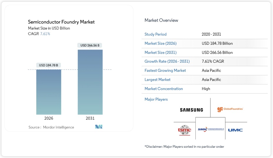
世界の半導体ファウンドリ市場規模は、2026年には1,847億8,000万米ドルに達すると推定されており、2025年の1,717億2,000万米ドルから拡大しています。2031年には2,665億6,000万米ドルに達すると予測されており、2026年から2031年にかけて年平均成長率(CAGR)7.61%で成長します。サブ5nmでの人工知能(AI)コンピューティング需要の急増、成熟ノードの車載用チップに対する持続的な需要、そして政府の強力なインセンティブが相まって、この分野の技術面と地理的フットプリントの双方が拡大しています。チップレットや3D ICをはじめとする高度なパッケージングは、収益の二大原動力となっていますが、水資源管理、輸出規制への対応、EUVツールの人材不足といった問題が、短期的な生産能力の増強を抑制しています。地政学的競争の激化により、北米、欧州、インドは製造の現地化を迫られており、アジア太平洋地域の伝統的な生産における優位性は徐々に薄れつつありますが、そのリーダーシップは揺るぎないものとなっています。現在、競争の動向は、5 nm 未満のノードにおけるリーダーシップ、コスト効率の高い 28 nm の容量、および新興企業をターゲットとしたサービスとしてのファウンドリの提供に左右されています。
Semiconductor Foundry Market Analysis
The global semiconductor foundry market size in 2026 is estimated at USD 184.78 billion, growing from 2025 value of USD 171.72 billion with 2031 projections showing USD 266.56 billion, growing at 7.61% CAGR over 2026-2031. A combination of soaring artificial-intelligence compute needs at sub-5 nm, sustained demand for mature-node automotive chips, and intensive government incentives is widening both the technology and geographic footprint of the sector. Advanced packaging, especially chiplets and 3-D ICs, has become a parallel revenue engine, while water stewardship, export-control compliance, and EUV-tool talent shortages temper near-term capacity additions. Intensifying geopolitical competition is prompting North America, Europe, and India to localize fabrication, gradually diffusing Asia-Pacific’s traditional production dominance without dislodging its leadership. Competitive dynamics now hinge on node leadership below 5 nm, cost-efficient 28 nm capacity, and foundry-as-a-service offerings targeting start-ups.
Global Semiconductor Foundry Market Trends and Insights
AI Accelerator Race for Less than 5 nm Advanced Nodes
Sub-5 nm capacity has moved from niche to mainstream as hyperscalers and chip designers race to train larger AI models. TSMC reported that 7 nm and finer nodes contributed 74% of wafer revenue in Q2 2025, underscoring the premium customers place on density leadership. Samsung’s gate-all-around 2 nm program and Intel’s 1.4 nm roadmap confirm an industry-wide pivot toward atomic-scale geometries. Rapid node migration is also fueling demand for advanced interposers, necessitating co-optimized fab and packaging lines. High capital intensity—often above USD 20 billion per fab—limits viable competitors and cements an oligopolistic market where process leadership directly dictates share.
Mainstream Chip Demand from Automotive Electrification
Electric vehicles require dual-track silicon: power-management ICs at mature nodes and high-compute SoCs at leading nodes. Automakers’ shift to centralized electronic architectures locks in long-term 28 nm and 45 nm volumes, providing reliable backfill for fabs otherwise pressured by cyclical smartphone orders. Long qualification cycles and strict AEC-Q100 standards encourage multi-year capacity reservations, improving revenue visibility for foundries that balance mature and advanced nodes. Tesla’s custom chip strategy illustrates how OEMs use dedicated capacity deals to secure supply and differentiate performance.
Geopolitical Export-Control Uncertainty
Expanded Foreign-Produced Direct Product rules restrict advanced lithography exports to specific countries, forcing fabs to segregate legacy and cutting-edge lines. Compliance costs rise as companies duplicate equipment sets and audits across jurisdictions. Malaysia’s tighter chip policies under U.S. pressure show knock-on effects in Southeast Asia, where routing high-end GPUs now triggers lengthy license reviews. Unpredictable rule-making discourages green-field projects, particularly at 5 nm and below, muting near-term investment cycles.
Other drivers and restraints analyzed in the detailed report include:
- Defense Agencies’ Push for Trusted Domestic Fabs
- Chiplets + 3-D IC Needing New Foundry Workflows
- Talent Crunch in Sub-3 nm EUV Maintenance
For complete list of drivers and restraints, kindly check the Table Of Contents.
Segment Analysis
In 2025, the 28 nm node generated 59.45% revenue, anchoring the semiconductor foundry market size for cost-sensitive, high-volume devices. Nodes finer than 10 nm, although smaller in shipment volume, will produce a 9.05% CAGR through 2031, reflecting AI and HPC pull-through. Revenue mix therefore bifurcates: mature nodes assure predictable automotive and industrial cash flows, while leading-edge nodes command premium pricing and margins.
Capex discipline remains pivotal. TSMC begins 2 nm risk production in 2025, drawing prepayments from smartphone and accelerator clients. Intel and Samsung respond with 1.4 nm and 2 nm gate-all-around timelines, intensifying capital races. Meanwhile, 16 nm and 14 nm nodes bridge cost-performance gaps for networking silicon. Legacy 65 nm and above still serve analog and RF designs with long lifecycles, keeping fabs running at healthy utilization even when handset demand softens.
The transition to 300 mm tooling lifted die output per run and cut edge-loss waste, enabling the segment to capture 68.10% of the semiconductor foundry market share in 2025. Growth persists at 9.42% CAGR as new fabs select 300 mm equipment by default for anything below 40 nm. In contrast, 200 mm remains entrenched in MEMS, power GaN, and niche analog where geometry or chemistry complicates 300 mm migration.
Economies of scale are stark. A 300 mm fab reaching 100,000 wafers-per-month can undercut 200 mm cost per die by 30% once fully depreciated. Yet the USD 15–20 billion entry fee restricts newcomers, reinforcing incumbent advantage. Specialized 150 mm lines persist for SiC, GaAs, and photonics products that rely on exotic substrates.
The Semiconductor Foundry Market Report is Segmented by Technology Node (10/7/5 Nm and Below, 16/14 Nm, 20 Nm, and More), Wafer Size (300 Mm, 200 Mm, ≤150 Mm), Foundry Business Model (Pure-Play, IDM Foundry Services, Fab-Lite), Application (Consumer Electronics and Communication, Automotive, and More), and Geography (North America, South America, Europe, and More). The Market Forecasts are Provided in Terms of Value (USD).
Geography Analysis
Asia-Pacific captured 22.65% revenue in 2025 and is set for an 8.44% CAGR through 2031, propelled by Taiwan’s unrivaled advanced-node density and South Korea’s vertical integration ecosystems. Taiwan’s Q2 2025 revenue of USD 28.87 billion underscores the region’s throughput scale. China’s SMIC concentrates on 28 nm and above amid export-tool restrictions, while Malaysia and Singapore reinforce assembly and test depth despite tighter U.S. compliance rules.
North America is re-emerging as a fabrication hub under the CHIPS Act, with groundbreakings in Arizona, Ohio, and New York adding both 5 nm class and mature-node capacity. Federal grants de-risk billion-dollar projects, and defense offsets guarantee baseline loadings. Europe focuses on automotive-grade and specialty analog, leveraging Germany’s auto cluster and the Netherlands’ lithography prowess. EU funding pools, though smaller than U.S. packages, aim to double regional output by 2030.
India, the Middle East, and pockets of Africa are staking claims via assembly, test, and design-service incentives. India’s USD 10 billion program attracted Micron’s USD 2.75 billion ATMP and Tata’s USD 11 billion green-field fab plans, targeting domestic demand approaching USD 100-110 billion by 2030. Gulf countries explore foundries for economic diversification, but water constraints and skills gaps temper speed. Collectively, new geographies aim to shorten supply chains and hedge geopolitical shocks.
List of Companies Covered in this Report:
- Taiwan Semiconductor Manufacturing Co. Ltd. (TSMC)
- Samsung Electronics Co. Ltd. (Samsung Foundry)
- GlobalFoundries Inc.
- United Microelectronics Corp. (UMC)
- Semiconductor Manufacturing International Corp. (SMIC)
- Intel Corp. (Intel Foundry Services)
- Tower Semiconductor Ltd.
- STMicroelectronics N.V.
- Powerchip Semiconductor Manufacturing Corp. (PSMC)
- Vanguard International Semiconductor Corp.
- Hua Hong Semiconductor Ltd.
- X-FAB Silicon Foundries SE
- ASE Group
- Dongbu HiTek Co. Ltd.
- Renesas Electronics Corp.
- JCET Group
- Amkor Technology
- SkyWater Technology Inc.
- VIS Semiconductor Co. Ltd.
- PSMC Group (Nexchip)
Additional Benefits:
- The market estimate (ME) sheet in Excel format
- 3 months of analyst support
Table of Contents
1 INTRODUCTION
1.1 Study Assumptions and Market Definition
1.2 Scope of the Study
2 RESEARCH METHODOLOGY
3 EXECUTIVE SUMMARY
4 MARKET LANDSCAPE
4.1 Market Overview
4.2 Market Drivers
4.2.1 Mainstream chip demand from automotive electrification
4.2.2 IoT-edge proliferation requiring mature?node capacity
4.2.3 AI accelerator race for Less than 5 nm advanced nodes
4.2.4 Chiplets + 3D IC needing new foundry workflows
4.2.5 Defense agencies push for trusted domestic fabs
4.2.6 Foundry-as-a-Service model for start-ups
4.3 Market Restraints
4.3.1 Geopolitical export-control uncertainty
4.3.2 Capex inflation and long pay-back periods
4.3.3 Water-use permits limiting mega-fabs
4.3.4 Talent crunch in sub-3 nm EUV maintenance
4.4 Industry Value Chain Analysis
4.5 Regulatory Landscape
4.6 Technological Outlook
4.7 Foundry Capacity Utilization Trends
4.8 Porter’s Five Forces Analysis
4.8.1 Bargaining Power of Suppliers
4.8.2 Bargaining Power of Buyers
4.8.3 Threat of New Entrants
4.8.4 Threat of Substitutes
4.8.5 Intensity of Competitive Rivalry
4.9 Impact of Macroeconomic Factors on the Market
5 MARKET SIZE AND GROWTH FORECASTS (VALUE)
5.1 By Technology Node
5.1.1 10/7/5 nm and below
5.1.2 16/14 nm
5.1.3 20 nm
5.1.4 28 nm
5.1.5 45/40 nm
5.1.6 65 nm and above
5.2 By Wafer Size
5.2.1 300 mm
5.2.2 200 mm
5.2.3 ?150 mm
5.3 By Foundry Business Model
5.3.1 Pure-play
5.3.2 IDM Foundry Services
5.3.3 Fab-lite
5.4 By Application
5.4.1 Consumer Electronics and Communication
5.4.2 Automotive
5.4.3 Industrial and IoT
5.4.4 High-Performance Computing (HPC)
5.4.5 Other Applications
5.5 By Geography
5.5.1 North America
5.5.1.1 United States
5.5.1.2 Canada
5.5.1.3 Mexico
5.5.2 South America
5.5.2.1 Brazil
5.5.2.2 Argentina
5.5.2.3 Rest of South America
5.5.3 Europe
5.5.3.1 Germany
5.5.3.2 United Kingdom
5.5.3.3 France
5.5.3.4 Italy
5.5.3.5 Rest of Europe
5.5.4 Asia-Pacific
5.5.4.1 China
5.5.4.2 Japan
5.5.4.3 South Korea
5.5.4.4 India
5.5.4.5 Rest of Asia-Pacific
5.5.5 Middle East
5.5.5.1 Saudi Arabia
5.5.5.2 United Arab Emirates
5.5.5.3 Rest of Middle East
5.5.6 Africa
5.5.6.1 South Africa
5.5.6.2 Rest of Africa
6 COMPETITIVE LANDSCAPE
6.1 Market Concentration
6.2 Strategic Moves
6.3 Market Share Analysis
6.4 Company Profiles (includes Global level Overview, Market level Overview, Core Segments, Financials as available, Strategic Information, Market Rank/Share, Products and Services, Recent Developments)
6.4.1 Taiwan Semiconductor Manufacturing Co. Ltd. (TSMC)
6.4.2 Samsung Electronics Co. Ltd. (Samsung Foundry)
6.4.3 GlobalFoundries Inc.
6.4.4 United Microelectronics Corp. (UMC)
6.4.5 Semiconductor Manufacturing International Corp. (SMIC)
6.4.6 Intel Corp. (Intel Foundry Services)
6.4.7 Tower Semiconductor Ltd.
6.4.8 STMicroelectronics N.V.
6.4.9 Powerchip Semiconductor Manufacturing Corp. (PSMC)
6.4.10 Vanguard International Semiconductor Corp.
6.4.11 Hua Hong Semiconductor Ltd.
6.4.12 X-FAB Silicon Foundries SE
6.4.13 ASE Group
6.4.14 Dongbu HiTek Co. Ltd.
6.4.15 Renesas Electronics Corp.
6.4.16 JCET Group
6.4.17 Amkor Technology
6.4.18 SkyWater Technology Inc.
6.4.19 VIS Semiconductor Co. Ltd.
6.4.20 PSMC Group (Nexchip)
7 MARKET OPPORTUNITIES AND FUTURE OUTLOOK
7.1 White-space and Unmet-need Assessment