Dicing Equipment - Market Share Analysis, Industry Trends & Statistics, Growth Forecasts (2026 - 2031)
ダイシング装置市場レポートは、ダイシング技術 (ブレードダイシング、レーザーアブレーション、ステルスダイシングなど)、ウェーハサイズ (150 mm以下、200 mm、300 mmなど)、アプリケーション (ロジックおよびメモリ、MEMSデバイス、パワーデバイス、CMOSイメージセンサーなど)、エンドユーザー産業 (ファウンドリ、IDMS、OSAT)、および地域別にセグメント化されています。
The Dicing Equipment Market Report is Segmented by Dicing Technology (Blade Dicing, Laser Ablation, Stealth Dicing, and More), Wafer Size (Less Than Equal To 150 Mm, 200 Mm, 300 Mm, and More) Application (Logic and Memory, MEMS Devices, Power Devices, CMOS Image Sensors, and More), End-User Industry (Foundries, Idms, and OSATs) and Geography.
| 出版 | Mordor Intelligence |
| 出版年月 | 2026年02月 |
| ページ数 | 137 |
| 価格 | 記載以外のライセンスについてはお問合せください |
| シングルユーザ | USD 4,750 |
| 種別 | 英文調査報告書 |
| 商品番号 | SMR-1465814658 |

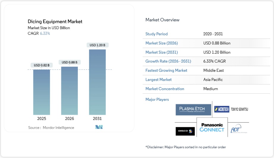
ダイシング装置市場規模は2026年には8億8,000万米ドルと推定され、2025年の8億3,000万米ドルから拡大し、2031年には12億米ドルに達すると予測され、2026年から2031年にかけて6.33%のCAGRで成長する見込みです。半導体バックエンド製造、特に薄型ウェーハ、先進的なパッケージングフォーマット、ワイドバンドギャップパワーデバイスへの旺盛な投資が、この着実な拡大を支えています。電気自動車、再生可能エネルギー、AIのワークロードが増大するにつれ、チップメーカーは高歩留まりのダイシンギュレーションを優先し、サブミクロンの位置決め精度、汚染制御処理、統合検査を組み合わせたシステムを支持しています。3Dおよびヘテロジニアスインテグレーションへの継続的な移行により、チッピングを最小限に抑え、より狭いストリートを可能にするプラズマおよびレーザーダイシングツールの需要が高まっています。一方、自動化のアップグレードは、工場における労働力の制約を相殺し、段取り替え時間を短縮し、総合設備効率を向上させるのに役立ちます。米国、欧州、東アジアにおけるサプライチェーンのローカリゼーション プログラムにより、新たな地域需要拠点が導入されていますが、希土類レーザー ソースをめぐる地政学的摩擦が根強く、スラリー廃棄に関する厳格な規則もあって、資本集約度は高いままとなっています。
セグメント分析
- ブレードシステムは、2025年にはダイシング装置市場の46.10%を占め、ウェーハエッジ単価の低さと成熟したサービスネットワークは、ロジックおよびメモリの量産ラインに適しています。しかし、50µm以下のウェーハの普及に伴い、従来のブレードでは保証できないカーフフリーのシンギュレーションが求められるようになり、レーザーセグメントは年平均成長率6.53%で拡大しています。パナソニックのAPX300プラズマプラットフォームは、300mmウェーハで20µmストリートを実現し、プラズマツールとレーザーツールの飛躍的な性能向上を裏付けています。ブレード粗加工とレーザー仕上げを組み合わせたハイブリッドラインも普及が進み、スループットとダイ強度のバランスを実現しています。
- レーザー光学系、希土類アライメント部品、数kW電源などの追加コストは、価格に敏感なファブでの導入を依然として制限しています。しかし、ダイ・トゥ・パッケージの垂直配線や脆いSiC基板が主流となっている場合、初期投資額の増加は、スクラップの減少と設計ルールの厳格化によって相殺されます。予測期間中、超高速パルス整形とオートフォーカス光学系の継続的な研究開発により、ツールのデューティサイクルが向上し、ウェーハ1枚あたりのコスト差が徐々に縮小すると予想されます。
- 半導体業界はウェーハの大口径化を進めており、450mmを超えるウェーハは2031年まで年平均成長率6.38%で成長すると予測されています。これは、2025年に37.55%の市場シェアを占めていた300mmウェーハに迫る規模です。特にパネルレベルパッケージングワークフローにおける高度なパッケージングアプリケーションは、より大きな基板処理能力への需要を促進しています。ディスコ社のDFD6370は、最大330×330mmのワークピースに対応し、従来のウェーハ処理と新たな大型フォーマットの要件との間のギャップを埋めます。
- 200mm以下のウェーハサイズを含む小型ウェーハは、MEMSデバイスやパワー半導体などの特殊用途において、基板コストとプロセス最適化の観点から既存のウェーハフォーマットが有利となるため、依然として重要な位置を占めています。200mmセグメントは成熟ノードの拡大と車載半導体の需要の恩恵を受けており、150mmウェーハは化合物半導体やレガシーデバイス製造といったニッチな用途に利用されています。しかし、基板あたりのダイ歩留まり向上やユニットあたりの処理コスト削減など、大型ウェーハの経済的メリットが、フォーマットの移行を促進しています。SEMIのWorld Fab Forecastでは、2027年までに稼働開始の可能性の高い79のファブが特定されており、その多くは複数のウェーハサイズに対応しています。単一プラットフォームで複数のウェーハフォーマットに対応するスケーラブルなハンドリングシステムを開発している装置サプライヤーは、この進化する市場において優位な立場にあります。
- ダイシング装置市場レポートは、ダイシング技術 (ブレードダイシング、レーザーアブレーション、ステルスダイシングなど)、ウェーハサイズ (≤ 150 mm、200 mm、300 mmなど)、アプリケーション (ロジックおよびメモリ、MEMSデバイス、パワーデバイス、CMOSイメージセンサーなど)、エンドユーザー産業 (ファウンドリ、IDMS、OSAT)、および地域 (北米、ヨーロッパ、アジア太平洋など) 別にセグメント化されています。
Dicing Equipment Market Analysis
Dicing equipment market size in 2026 is estimated at USD 0.88 billion, growing from 2025 value of USD 0.83 billion with 2031 projections showing USD 1.2 billion, growing at 6.33% CAGR over 2026-2031. Robust investment in semiconductor backend manufacturing, especially for thinner wafers, advanced packaging formats, and wide-bandgap power devices, underpins this steady expansion. As electric-vehicle, renewable-energy, and AI workloads intensify, chipmakers prioritize high-yield die singulation, favoring systems that combine sub-micrometer positioning accuracy, contamination-controlled processing, and integrated inspection. Continuous migration toward 3D and heterogeneous integration is elevating the demand for plasma and laser dicing tools that minimize chipping and enable narrower streets. Meanwhile, automation upgrades help fabs offset labor constraints, shorten changeover times, and boost overall equipment effectiveness. Supply-chain localization programs in the United States, Europe, and East Asia introduce new regional demand nodes; however, persistent geopolitical frictions surrounding rare-earth laser sources and stringent slurry-disposal rules continue to keep capital intensity high.
Global Dicing Equipment Market Trends and Insights
Technological Advancements in High-Precision Motion Systems
Recent motion-control breakthroughs deliver sub-micrometer stage accuracy essential for heterogeneous integration lines. DISCO’s DFD6370 platform, for instance, handles 330 × 330 mm substrates while using selectable height sensors that keep cut depth within ±1 µm, an advantage for panel-level packaging. Active damping, closed-loop robotics, and vision-guided alignment further trim vibration and thermal drift, enabling higher yield when processing brittle silicon-carbide wafers. Vendors integrating multi-axis stages with on-board metrology now offer turnkey singulation cells that combine cutting, cleaning, and inspection in a single flow, reducing handling defects and cycle time.
Surge in Demand from Advanced Logic and Memory Fabs
SEMI projects cumulative 300 mm fab equipment outlays to reach USD 400 billion between 2025 and 2027, with foundries accounting for USD 230 billion of that total. New extreme-ultraviolet nodes and 3D-stacked DRAM lines magnify backside contamination risks, prompting fabs to specify dicing tools with electrostatic-charge suppression and hermetic chip-collection. As capacity ramps accelerate, particularly at TSMC, Samsung, and China’s domestic foundries, rapid tool delivery and field-service reach become procurement gatekeepers for equipment suppliers.
Stricter Slurry/Chemical Disposal Regulations
ISO 14644 cleanroom revisions and emerging PFAS controls require fabs to retrofit wastewater loops, install fluorinated-compound abatement systems, and adopt closed-loop coolants.Vendors that embed recycling modules and real-time particulate monitors inside dicing cells help customers meet regulatory thresholds while reducing utility bills; however, the added equipment cost and facility retrofit delay some purchase decisions.
Other drivers and restraints analyzed in the detailed report include:
- Rapid Adoption of 3D Packaging and Heterogeneous Integration
- Growing Deployment of Power Devices for EV and Renewables
- Laser Source Supply Bottlenecks and Rare-Earth Dependency
For complete list of drivers and restraints, kindly check the Table Of Contents.
Segment Analysis
Blade systems controlled 46.10% of the dicing equipment market in 2025, their cost-per-wafer edge and mature service networks suiting high-volume logic and memory lines. However, the laser segment is expanding at a 6.53% CAGR as sub-50 µm wafers proliferate, requiring kerf-free singulation that conventional blades cannot guarantee. Panasonic’s APX300 plasma platform enables 20 µm streets on 300 mm wafers, underscoring the performance leap plasma and laser tools deliver. Hybrid lines that combine blade rough-cutting with laser finishing are also gaining traction, striking a balance between throughput and die strength.
The incremental cost of laser optics, rare-earth alignment components, and multi-kW power supplies still limits adoption in price-sensitive fabs. Yet where die-to-package vertical interconnect or brittle SiC substrates prevail, the higher upfront spend is offset by lower scrap and tighter design rules. Over the forecast horizon, sustained research and development in ultrafast pulse shaping and auto-focus optics is expected to enhance tool duty cycle, gradually narrowing the per-wafer cost gap.
The semiconductor industry is transitioning to larger wafer formats, with wafers exceeding 450 mm projected to grow at a 6.38% CAGR through 2031, challenging the 300 mm wafers, which held a 37.55% market share in 2025. Advanced packaging applications, particularly in panel-level packaging workflows, are driving demand for larger substrate-handling capabilities. DISCO Corporation’s DFD6370 supports workpieces up to 330 × 330 mm, addressing the gap between conventional wafer processing and emerging large-format requirements.
Smaller wafer sizes, including 200 mm and below, remain relevant in specialized applications such as MEMS devices and power semiconductors, where substrate costs and process optimization favor established formats. The 200 mm segment benefits from mature node expansion and automotive semiconductor demand, while 150 mm wafers serve niche applications in compound semiconductors and legacy device production. However, the economic advantages of larger wafers, including higher die yield per substrate and reduced per-unit processing costs, are driving format migration. SEMI’s World Fab Forecast identifies 79 high-probability facilities beginning operations through 2027, many incorporating mixed wafer-size capabilities. Equipment suppliers developing scalable handling systems for multiple wafer formats within single platforms are well-positioned for this evolving landscape.
The Dicing Equipment Market Report is Segmented by Dicing Technology (Blade Dicing, Laser Ablation, Stealth Dicing, and More), Wafer Size (≤ 150 Mm, 200 Mm, 300 Mm, and More) Application (Logic and Memory, MEMS Devices, Power Devices, CMOS Image Sensors, and More), End-User Industry (Foundries, Idms, and OSATs) and Geography (North America, Europe, Asia-Pacific, and More). The Market Forecasts are Provided in Terms of Value (USD).
Geography Analysis
The Asia-Pacific region retained a 42.55% share of the dicing equipment market in 2025, driven by its deep-seated manufacturing clusters across Taiwan, South Korea, Japan, and mainland China. Tokyo-backed subsidies totaling JPY 3.9 trillion (USD 0.026 trillion) underpin Japan’s resurgence, channeling orders to precision-motion vendors and automation integrators. Chinese OSATs accelerate plasma-dicing line installs to raise yields on locally designed AI accelerators, while Southeast Asian nations attract assembly spillover, spawning mid-tier blade-dicer demand.
North America’s CHIPS Act has unlocked more than USD 50 billion in incentives, transforming greenfield fabs in Arizona, Texas, and upstate New York into new procurement hubs starting in 2026. These sites prioritize fully automated blade and laser cells, equipped with predictive maintenance analytics, to offset skilled labor shortages.
Europe’s Chips Act funnels USD 47 billion into continental capacity, led by German and French projects focused on silicon-carbide power electronics for EV supply chains. Although smaller than Asian volumes, the stringent environmental standards in EU fabs accelerate uptake of closed-loop slurry and low-water-consumption plasma dicing systems, nudging regional ASPs upward.
List of Companies Covered in this Report:
- DISCO Corporation
- Tokyo Seimitsu Co., Ltd. (ACCRETECH)
- Advanced Dicing Technologies Ltd.
- Panasonic Connect Co., Ltd.
- SPTS Technologies Ltd. (KLA Corporation)
- Plasma-Therm LLC
- Veeco Instruments Inc.
- Synova SA
- 3D-Micromac AG
- Han’s Laser Technology Industry Group Co., Ltd.
- Suzhou Delphi Laser Co., Ltd.
- EO Technics Co., Ltd.
- Neon Tech Co., Ltd.
- ASM Laser Separation International B.V.
- Kulicke & Soffa Industries, Inc.
- Takatori Corporation
- Lumentum Holdings Inc. (dicing lasers)
- IPG Photonics Corporation
- Oxford Instruments Plasma Technology
- Plasma Etch Inc.
- Dynatex International
- Loadpoint Micro Machining Ltd.
- Disco Hi-Tec America, Inc.
- Shenzhen JLH Laser Co., Ltd.
- Wuhan HGLaser Engineering Co., Ltd.
Additional Benefits:
- The market estimate (ME) sheet in Excel format
- 3 months of analyst support
Table of Contents
1 INTRODUCTION
1.1 Study Assumptions and Market Definition
1.2 Scope of the Study
2 RESEARCH METHODOLOGY
3 EXECUTIVE SUMMARY
4 MARKET LANDSCAPE
4.1 Market Overview
4.2 Market Drivers
4.2.1 Technological advancements in high-precision motion systems
4.2.2 Surge in demand from advanced logic and memory fabs
4.2.3 Rapid adoption of 3D packaging and heterogeneous integration
4.2.4 Growing deployment of power devices for EV and renewables
4.2.5 Shift toward plasma dicing for ultra-thin wafers
4.2.6 Localization incentives for domestic equipment in China
4.3 Market Restraints
4.3.1 High capital expenditure and long pay-back period
4.3.2 Yield losses from chipping and micro-cracks
4.3.3 Stricter slurry/chemical disposal regulations
4.3.4 Laser source supply bottlenecks and rare-earth dependency
4.4 Impact of Macroeconomic Factors on the Market
4.5 Industry Supply Chain Analysis
4.6 Regulatory Landscape
4.7 Technological Outlook
4.8 Porter’s Five Forces Analysis
4.8.1 Threat of New Entrants
4.8.2 Bargaining Power of Buyers/Consumers
4.8.3 Bargaining Power of Suppliers
4.8.4 Threat of Substitute Products
4.8.5 Intensity of Competitive Rivalry
5 MARKET SIZE AND GROWTH FORECASTS (VALUE)
5.1 By Dicing Technology
5.1.1 Blade Dicing
5.1.2 Laser Ablation
5.1.3 Stealth Dicing
5.1.4 Plasma Dicing
5.2 By Wafer Size
5.2.1 ≤ 150 mm
5.2.2 200 mm
5.2.3 300 mm
5.2.4 ≥ 450 mm
5.3 By Application
5.3.1 Logic and Memory
5.3.2 MEMS Devices
5.3.3 Power Devices
5.3.4 CMOS Image Sensors
5.3.5 RFID / Smart Cards
5.4 By End-User Industry
5.4.1 Foundries
5.4.2 IDMs
5.4.3 OSATs
5.5 By Geography
5.5.1 North America
5.5.1.1 United States
5.5.1.2 Canada
5.5.1.3 Mexico
5.5.2 South America
5.5.2.1 Brazil
5.5.2.2 Argentina
5.5.2.3 Rest of South America
5.5.3 Europe
5.5.3.1 Germany
5.5.3.2 United Kingdom
5.5.3.3 France
5.5.3.4 Italy
5.5.3.5 Spain
5.5.3.6 Russia
5.5.3.7 Rest of Europe
5.5.4 Asia-Pacific
5.5.4.1 China
5.5.4.2 Japan
5.5.4.3 India
5.5.4.4 South Korea
5.5.4.5 South-East Asia
5.5.4.6 Rest of Asia-Pacific
5.5.5 Middle East and Africa
5.5.5.1 Middle East
5.5.5.1.1 Saudi Arabia
5.5.5.1.2 United Arab Emirates
5.5.5.1.3 Rest of Middle East
5.5.5.2 Africa
5.5.5.2.1 South Africa
5.5.5.2.2 Egypt
5.5.5.2.3 Rest of Africa
6 COMPETITIVE LANDSCAPE
6.1 Market Concentration
6.2 Strategic Moves
6.3 Market Share Analysis
6.4 Company Profiles (includes Global level Overview, Market level overview, Core Segments, Financials as available, Strategic Information, Market Rank/Share for key companies, Products and Services, and Recent Developments)
6.4.1 DISCO Corporation
6.4.2 Tokyo Seimitsu Co., Ltd. (ACCRETECH)
6.4.3 Advanced Dicing Technologies Ltd.
6.4.4 Panasonic Connect Co., Ltd.
6.4.5 SPTS Technologies Ltd. (KLA Corporation)
6.4.6 Plasma-Therm LLC
6.4.7 Veeco Instruments Inc.
6.4.8 Synova SA
6.4.9 3D-Micromac AG
6.4.10 Han’s Laser Technology Industry Group Co., Ltd.
6.4.11 Suzhou Delphi Laser Co., Ltd.
6.4.12 EO Technics Co., Ltd.
6.4.13 Neon Tech Co., Ltd.
6.4.14 ASM Laser Separation International B.V.
6.4.15 Kulicke & Soffa Industries, Inc.
6.4.16 Takatori Corporation
6.4.17 Lumentum Holdings Inc. (dicing lasers)
6.4.18 IPG Photonics Corporation
6.4.19 Oxford Instruments Plasma Technology
6.4.20 Plasma Etch Inc.
6.4.21 Dynatex International
6.4.22 Loadpoint Micro Machining Ltd.
6.4.23 Disco Hi-Tec America, Inc.
6.4.24 Shenzhen JLH Laser Co., Ltd.
6.4.25 Wuhan HGLaser Engineering Co., Ltd.
7 MARKET OPPORTUNITIES AND FUTURE OUTLOOK
7.1 White-space and Unmet-Need Assessment